

 Deutsch
 Korean
PCB Design Cost Drivers

Why Design for Manufacturing Saves Money
At first glance, PCB costs seem easy to estimate: more layers increase cost, larger board sizes require more material – simple enough.
However, in practice, the most important cost drivers are not just layer count or board size. The biggest lever lies much earlier in the process: in the design itself.
In this article, we explain how factors such as layer count, trace widths, spacing, drill sizes, and special design features influence PCB costs.
Design for Manufacturing Determines Cost and Quality
PCBs are the backbone of modern electronics – and even small design decisions can have a major impact on cost and lead times.
Cost structures can vary significantly between manufacturers. This means that an increase in layer count does not always result in the same price increase.
- On average, costs may rise by 20–40% when increasing the number of layers. For example:
- A high-end PCB manufacturer might only increase costs by around 20% when moving from 8 to 10 layers
- A low-cost manufacturer may see increases of 35% or more
- Choosing the right manufacturing partner is therefore essential.
Important: Reducing the number of layers does not automatically reduce costs.
If fewer layers lead to a more complex design, overall costs may actually increase.
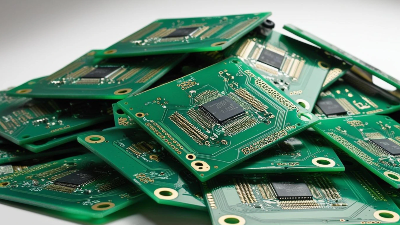
Complex PCB Designs and Their Cost Impact
HDI (High Density Interconnect) Technologies
HDI PCBs feature high wiring density and require more advanced manufacturing processes. As a result, they are typically more expensive.
Key cost drivers include:
- Fine trace geometries: Narrow traces and spacing (e.g. 75 µm with 100 µm copper) increase manufacturing complexity and cost.
- Controlled impedance: Requires precise stack-ups, tight tolerances, and additional testing. Extra processes and space for test coupons add cost.
- Microvias: Small vias used to connect layers. They often require advanced build-up processes and increase the number of lamination cycles. Note: In some cases, microvias can reduce costs by enabling fewer layers and thinner boards.
- Aspect ratio (via depth vs. diameter): High aspect ratios make plating more difficult. Many or very small drill holes increase cost.
- Plugged vias (filled and capped): Additional processing steps make this a cost-intensive solution.
- Buried vias / additional lamination cycles: Increase manufacturing complexity and cost.
- Mechanical tolerances: Deviations from standard tolerances (e.g. routing edges, cut-outs) increase effort and cost.
- Copper thickness in fine structures: Thick copper combined with fine geometries increases etching complexity and risk of defects.
- Gold thickness: Typically has only a minor impact on overall cost due to low material usage.
EVYTRA Recommendation
Every deviation from standard specifications increases manufacturing effort – and therefore cost.
To achieve cost-efficient and reliable designs:
- Focus on design for manufacturing (DfM) early in development
- Keep designs as close to standard as possible
- Minimize the number of lamination cycles where possible
- Align design decisions with manufacturing processes early on
As a general rule:
- Costs increase roughly in proportion to material usage and layer count
- Higher complexity and density lead to higher costs
Standards such as IPC-2220 and IPC-2226 provide valuable guidance for cost-efficient design.
Work Closely with Your Manufacturer
For more complex designs, it is essential to understand the manufacturing process in detail. We strongly recommend engaging with your PCB supplier early in the design phase.
At the same time, developers should stay up to date with new manufacturing technologies, as PCB production is continuously evolving.
Alternatively, working with an experienced partner ensures that cost optimization is already considered during the design phase.
Optimize Your PCB Costs
From design to manufacturing strategy – EVYTRA helps you identify efficiency potential at every stage.
Discover more cost-saving tips in our blog or get in touch to define your optimal PCB sourcing strategy.